
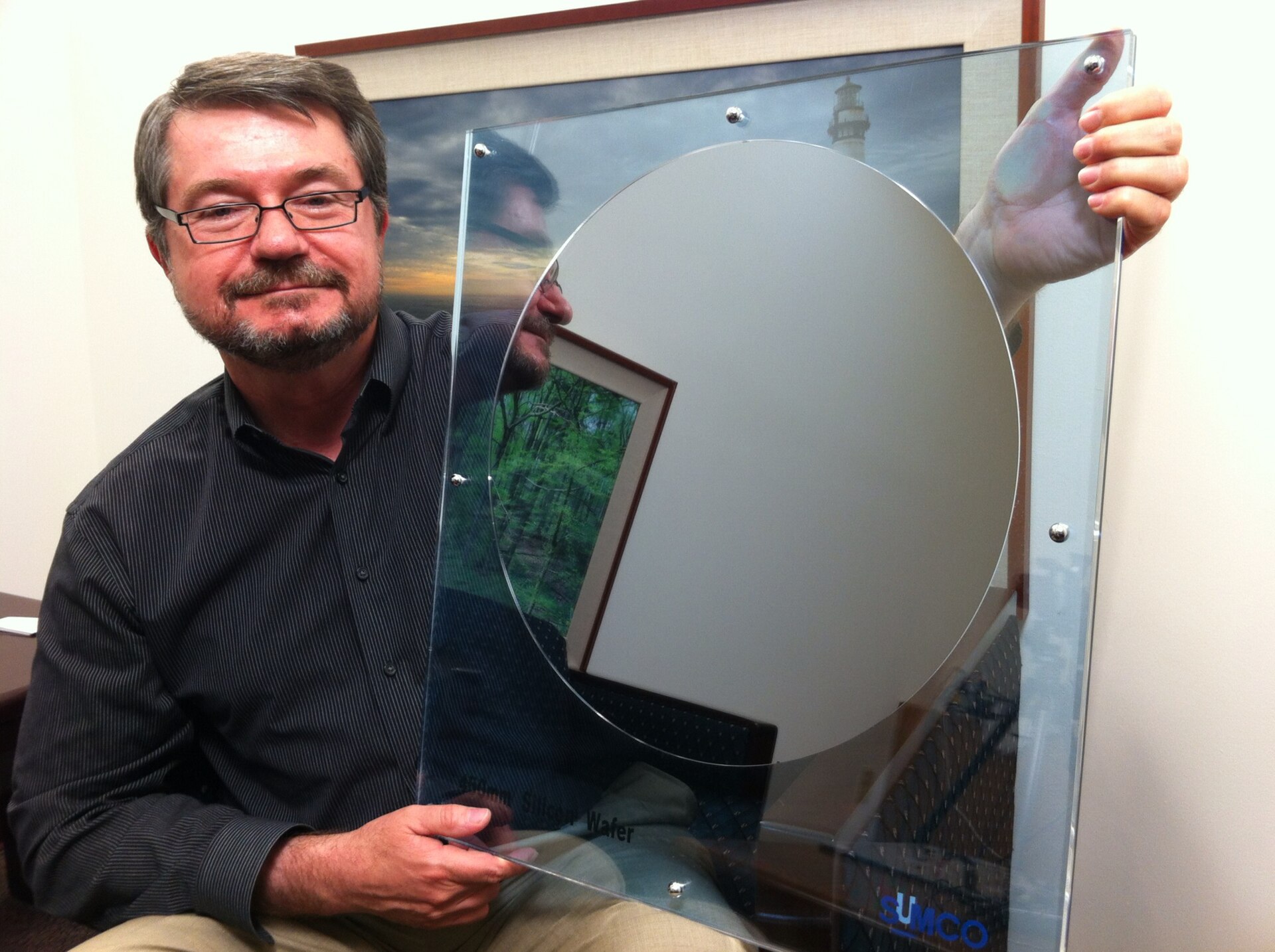
In the fourth quarter of 2025, TSMC quietly started volume production of its N2 process at Fab 22 near Kaohsiung, Taiwan. There was no launch event and no glossy video. The company simply updated its technology page to say that 2nm technology had entered volume production in 4Q25 as planned, and the semiconductor industry moved into a new transistor era.
That transition matters more than the usual node-to-node shrink. For roughly a decade, every leading-edge chip you have owned — the processor in your laptop, the system-on-chip in your phone, the GPUs training large language models — used a transistor shape called a FinFET. N2 is TSMC’s first process built on a different shape entirely: the gate-all-around nanosheet. Samsung got there first in 2022 and struggled. Intel arrived at roughly the same time as TSMC with its own version. All three are now betting their next decade on it.
Here is what actually changed inside the transistor, what the verified performance numbers say, who is building on N2, and why a 2nm wafer costs about $30,000.
What a gate-all-around nanosheet transistor actually is
A transistor is a switch. Current flows through a channel from a source to a drain, and a gate sitting on top of that channel decides whether the flow is on or off. The gate does this by applying an electric field. The more of the channel the gate physically surrounds, the more completely it controls that field — and the less current leaks through when the switch is supposed to be off.
Planar transistors, the flat kind used until about 2011, had the gate touching only one side of the channel. As channels got shorter, leakage became unmanageable. FinFETs fixed that by standing the channel up on its edge as a thin vertical “fin,” so the gate could wrap three sides of it.
A nanosheet transistor takes the last step. The channel becomes a set of thin horizontal ribbons of silicon, stacked vertically like shelves, and the gate material is grown completely around each ribbon — all four sides. That is the “gate-all-around” part. Intel calls its implementation RibbonFET; Samsung calls its version MBCFET, for multi-bridge channel FET. They are variations on the same idea.
Why FinFET ran out of road
The research institute imec has described the endgame clearly: shrinking FinFET-based standard cells relied on removing fins, going from three fins per cell down to two and then one. Fewer fins means less drive current and worse variability, and once you reach a single fin there is nowhere left to go.
Nanosheets break that constraint in two ways. First, stacking sheets vertically gives you more effective channel width in the same footprint than a single fin can. Second — and this is the part chip designers care about most — sheet width is a continuous design variable. A fin gives you drive current in fixed quantised steps. A nanosheet can be made wider for a high-performance block or narrower for a low-power, low-capacitance block. TSMC markets this flexibility as NanoFlex, and it is why the density gain from N2 varies so much depending on what kind of circuit you are building.
The verified N2 numbers
TSMC’s comparison baseline is N3E, its mainstream 3nm process. Against that baseline, N2 is quoted at 10–15% more performance at the same power, or 25–30% less power at the same performance. Density improves by about 1.15x for mixed designs containing logic, SRAM and analog, and by up to roughly 1.20x for logic-only blocks, according to figures reported when volume production began.
Read those numbers honestly. They are an either/or, not a both. A phone chip designer will spend most of the budget on the power side and take a modest clock bump. A data-centre designer running into a rack power ceiling will do the same thing for different reasons. Nobody gets 15% more speed and 30% less power simultaneously.
Also note what is missing: SRAM. Cache memory has scaled far worse than logic for several nodes now, which is a large part of why modern chips are broken into chiplets and why cache density is quietly becoming the limiting factor in CPU design.
| Node | Transistor type | Headline claim | Volume production |
|---|---|---|---|
| TSMC N2 | 1st-gen GAA nanosheet | 10–15% speed or 25–30% power vs N3E | Q4 2025 |
| TSMC N2P | 1st-gen GAA nanosheet | ~10% performance over N2 | Late 2026 into 2027 |
| TSMC A16 | GAA + Super Power Rail | 8–10% speed or 15–20% power vs N2P | 2027 (delayed from 2026) |
| Intel 18A | RibbonFET + PowerVia | Up to 15% perf/watt, 30% density vs Intel 3 | Q4 2025 |
| Samsung SF2 | MBCFET nanosheet | Used in Exynos 2600 | 2025–26 |
Where N2 is being made, and how fast it is ramping
Production began at Fab 22 in Kaohsiung, with Fab 20 near Hsinchu — next to TSMC’s main R&D campus — ramping alongside it. Both sites are running multiple phases in parallel, and TSMC has said further Fab 22 phases are being equipped through the second half of 2026. A 2nm-capable phase of Fab 21 in Phoenix, Arizona is under construction but is not expected to produce N2 until later this decade.
The ramp is real but still early. On TSMC’s Q2 2026 earnings call in July 2026, N2 accounted for 3% of wafer revenue, against 30% for N3 and 33% for N5. Everything at 7nm and below made up 77% of wafer revenue. CFO Wendell Huang warned that the steep 2nm ramp would dilute gross margin by roughly 3–4 percentage points in the second half of 2026 — the normal cost curve of a new node, where you are paying for equipment and yield learning before the revenue arrives.
Wafer costs and why they matter to you
Reports in late 2025 put N2 wafer pricing at around $30,000, roughly 10–20% above the $25,000–$27,000 range for 3nm wafers, according to supply-chain reporting compiled by TrendForce. That was notably below earlier speculation of a 50% jump. Wafers produced in Arizona reportedly carry an additional premium.
These are supply-chain figures, not published price lists, so treat them as approximate. But the direction is clear and it has a consumer consequence. A wafer yields a fixed number of dies. If wafer cost rises 15% and density rises 15%, cost per transistor is roughly flat — which is the historical bargain of Moore’s Law finally flattening out. You get better chips, not cheaper ones. That is a large part of why flagship phone prices have drifted upward and why AI accelerators cost what they do.
What comes after N2: N2P, A16 and backside power
N2P is the performance-tuned refresh of N2, still using conventional front-side power delivery. A16 is the more interesting step. It pairs the same first-generation nanosheet transistors with Super Power Rail, TSMC’s backside power delivery network.
Backside power solves a wiring problem. In a conventional chip, power and signals both compete for the metal layers stacked above the transistors. Power wires need to be fat to avoid voltage droop; signal wires need to be dense. Moving the power network to the back of the wafer and connecting it directly into the transistor source and drain frees the front side entirely for signals and cuts resistive voltage loss.
A VLSI 2026 paper summarised on SemiWiki credits A16 with 8–10% higher speed at the same power, 15–20% lower power at the same speed, and an 8–10% density gain relative to N2P.
Timing is where the story has shifted, and it is worth being blunt about it. N2P and A16 were originally slated for the second half of 2026. In an April 2026 roadmap update, TSMC moved A16 to 2027 and split its roadmap in two: an annual cadence of client and smartphone nodes, and a slower two-year cadence for AI and HPC nodes. A14 is targeted at 2028 with second-generation nanosheets, and A13 and A12 at 2029. Notably, TSMC has said none of those nodes require High-NA EUV lithography.
Some sources still cite Q4 2026 for A16 production. The company’s own roadmap update is the more recent and more authoritative signal, and it says 2027.
The competition: Intel 18A and Samsung SF2
Intel reached high-volume 2nm-class manufacturing at roughly the same time, at Fab 52 in Chandler, Arizona. Its 18A node combines RibbonFET gate-all-around transistors with PowerVia backside power — meaning Intel shipped backside power a generation earlier than TSMC will. Intel claims up to 15% better performance per watt and 30% better chip density versus Intel 3. Panther Lake, sold as Core Ultra series 3, went to broad availability in January 2026.
The caveat is economics rather than physics. Intel CFO David Zinsner has said 18A yields will not reach the company’s desired cost thresholds until the end of 2026 at the earliest. And analyst density estimates cited by Tom’s Hardware put 18A at around 238 million transistors per square millimetre for high-density cells against roughly 313 for N2 — though such comparisons are estimates, and backside power changes what the front side has to carry. Intel’s 14A, which introduces PowerDirect and is expected to use High-NA EUV, hinges on winning external foundry customers; CEO Lip-Bu Tan has pointed to decisions landing between late 2026 and the first half of 2027.
Samsung was first to gate-all-around at 3nm in 2022 but spent years fighting yield. Its SF2 process powers the Exynos 2600, announced in December 2025 as the first 2nm gate-all-around application processor, with up to 39% higher CPU performance than the Exynos 2500 and a claimed 113% uplift in generative-AI NPU performance. Reported yields have ranged from roughly 50% to 60% depending on the source and the month, and none of those figures are official.
Which products actually use it
- Apple is reported to have secured the bulk of TSMC’s initial 2nm capacity for its A20 series, aimed at the iPhone 18 generation and a foldable model. These are supply-chain reports from Taiwanese outlets, not Apple statements.
- Qualcomm and MediaTek are both competing for 2nm slots, with MediaTek having taped out a 2nm flagship SoC and targeted mass production for late 2026.
- AI and HPC silicon is the second wave. TSMC has said N2 demand is being driven by both smartphone and HPC/AI designs, and the A16 node with backside power is explicitly aimed at data centre parts.
- Intel’s own products — Panther Lake on the client side, Clearwater Forest on the server side — are the volume drivers for 18A.
What this means for you
If you are buying a phone or laptop, the practical effect of 2nm arrives as battery life more often than speed. A chip that can do the same work for 25–30% less power translates into longer screen-on time and less thermal throttling during sustained tasks — video calls, gaming, on-device AI. Expect the marketing to emphasise AI TOPS numbers; treat those as a separate claim from the process node, because NPU performance depends far more on architecture and memory bandwidth than on transistor shape.
If you are budgeting for AI compute, the node is not where your cost is going. Advanced packaging and high-bandwidth memory are the scarcer resources, and the $30,000 wafer is only one line in a much larger bill. A 2nm die does help — power per unit of compute is the binding constraint in data centres — but do not expect the price of inference to fall in step with transistor density.
If you are simply following the industry, the useful thing to watch is not who claims the smallest number. Node names stopped describing physical dimensions years ago. Watch yield commentary, watch which external customers commit, and watch whether backside power delivers in production what it promises on paper.
Frequently asked questions
Is a 2nm chip actually 2 nanometres across anything?
No. Node names have been marketing labels since roughly the 22nm generation. Nothing in an N2 or 18A transistor measures 2 nanometres. The names indicate roughly where a process sits on the industry’s scaling curve, which is why comparing TSMC, Intel and Samsung nodes by name alone is unreliable.
Is gate-all-around a bigger change than previous node shrinks?
Structurally, yes — it is the first new transistor architecture at the leading edge in about a decade. Commercially, the first generation delivers a normal full-node improvement. The larger payoff comes from second-generation nanosheets and from stacking devices vertically, which the industry calls CFET and is still years out.
Why is TSMC skipping High-NA EUV when Intel is not?
TSMC has said its nodes through 2029, including A12 and A13, do not require High-NA. Its position is that existing EUV with multipatterning remains more economical for now. Intel has bet on adopting High-NA earlier at 14A. Both bets are defensible and the industry genuinely disagrees about which is right.
Will 2nm make chips cheaper?
Not on a per-chip basis. Wafer cost is rising at roughly the same rate as density improves, so cost per transistor is close to flat. What you buy with 2nm is better performance per watt, not lower prices.
Should I wait for a 2nm phone or laptop?
Only if you are already due for an upgrade. The generational gain is real but incremental, and a well-designed 3nm device with good thermals will often outperform a poorly designed 2nm one in sustained workloads.
The part of the story still unwritten
Gate-all-around is now the industry standard, but it is the first generation of a structure meant to run for a decade. The interesting questions are the ones nobody can answer yet: whether Intel converts 18A’s technical parity into a foundry business with real external customers, whether Samsung’s yields close the gap enough to give buyers a genuine third option, and whether backside power delivers its promised gains once complex AI dies are running hot in production.
What is already settled is that the fin is gone. Every leading-edge chip designed from here forward is a nanosheet design, and the next architectural fight — forksheet, then CFET, then whatever follows — is already being simulated in research labs while the first 2nm phones reach store shelves.
Sources
- TSMC — 2nm Technology
- Tom’s Hardware — TSMC begins volume production of 2nm-class chips
- Tom’s Hardware — TSMC unveils process technology roadmap through 2029
- Tom’s Hardware — Analyzing TSMC’s fab expansion roadmap
- imec — Entering the nanosheet transistor era
- The Motley Fool — TSMC Q2 2026 earnings call transcript
- TrendForce — TSMC 2nm reportedly up 10–20%
- SemiWiki — TSMC A16 backside power at VLSI 2026
- Intel Newsroom — Intel unveils Panther Lake architecture built on 18A
- Tom’s Hardware — Intel’s roadmaps examined: 14A, Nova Lake, Diamond Rapids
- TrendForce — Samsung unveils Exynos 2600, first 2nm GAA AP
- TrendForce — Apple reportedly takes most of TSMC’s 2nm capacity
Image credit: Photo: Intel Free Press — CC BY 2.0 (via Wikimedia Commons)
